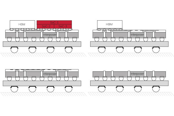
In the fast-changing world of semiconductors, the demand for precision, efficiency, and reliability is key. Chiplets and Advanced Packaging have a revolutionary impact on chip design and manufacturing by breaking down intricate integrated circuits into interconnected, specialized components. This approach brings many advantages, including enhanced flexibility, scalability, and cost-effectiveness in semiconductor design.
In this dynamic area, developments in bond testing techniques are paving the way for the next generation of bond testers, where automation plays a critical role in testing the quality of chiplets and ensuring a reliable and high-performance final product. We at xyztec, are proud to introduce groundbreaking advancements in automatic loading, testing, and analyzing that redefine the essence of chiplet evaluation. Here is a glimpse into the aspects that are reshaping the semiconductor industry:
Automatic grading
Auto grading of sheared bonds can be seen as a Semantic Segmentation problem. It is similar to solving a puzzle where each piece needs a label. In this case, it’s like assigning labels to every pixel in an image by giving a classification (e.g., Ductile, Brittle, Gold, etc.). This can be done fully automatically using a Deep Learning network.
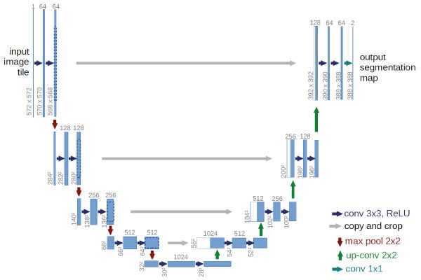
FIGURE 1: U-net architecture.
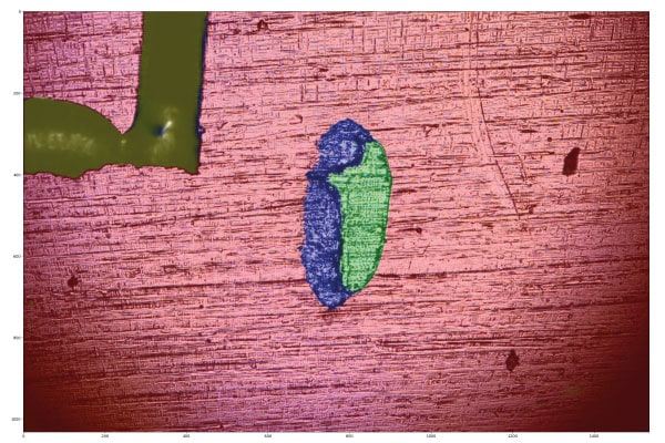
FIGURE 2: Image graded by trained U-Net2. (Sample: Thin wire shear, aluminum on aluminum, Melaka. Red: Background, Green: Ductile, Blue: Brittle, Yellow: Debris.
Precision in measurement and early detection
Image measurement is an additional function that is intended for further scientific approaches or is used for early detection. Our ongoing studies align images with precise measurements (FIGURE 4), aiming to detect and predict trends, enabling early warning systems for chiplets. The goal is to minimize errors, maximize efficiency, and fortify the production chain.
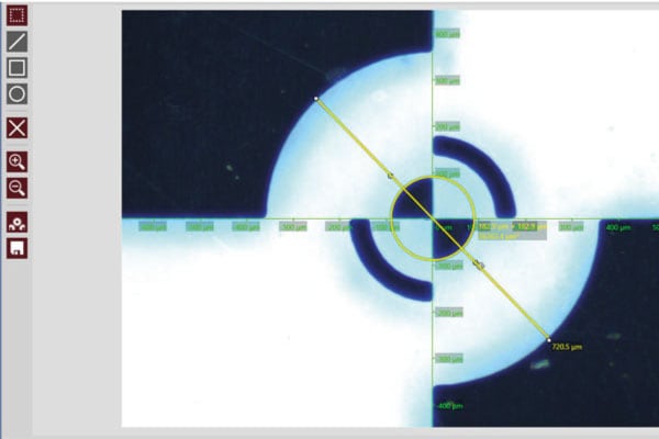
FIGURE 3: Calibration tool for image measurement.
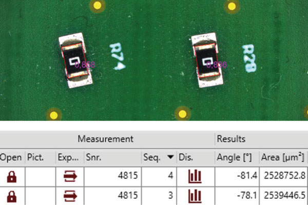
FIGURE 4: Image recognition with measurement.
Enhanced data management through wafer mapping
The meticulous marking and error-free data transfer through updated wafer format files (FIGURE 5) ensure comprehensive tracking of tests performed. Every tested sector is unmistakably identified, facilitating streamlined data communication with a vigilant eye on every step of the process.
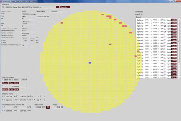
FIGURE 5: Wafer mapping with V marker.
Data communication SECS/GEM and GEM300
SECS/GEM and GEM300 are communication standards set by Semiconductor Equipment and Materials International (SEMI). They define a generic model for controlling production equipment, allowing remote control and automation supported by MES. These standards facilitate structured data collection, enabling better quality and availability. SECS/GEM follows a layered protocol architecture, facilitating various levels of data exchange and enabling information flow for monitoring and control (FIGURE 6).
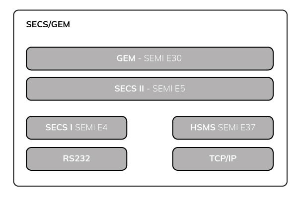
FIGURE 6: SECS GEM Organization.
Yet, for high-end production with automated material transport, the GEM300 standards become the cornerstone. Detailed tracking, control job differentiation, and in-depth performance monitoring within the system (FIGURE 7) ensure unparalleled control over the entire production process.
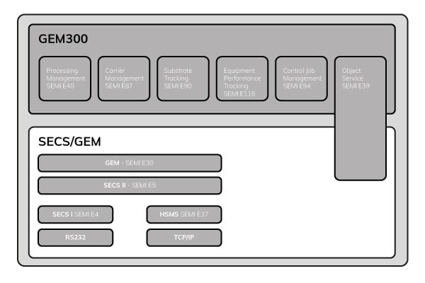
FIGURE 7: Communication interface.
Put it to the test!
Bond testing plays a crucial role in ensuring the quality and performance of chiplets. From evaluating the mechanical properties of the interconnect materials to analyzing the thermal behavior and electrical conductivity, precise and accurate testing is essential for achieving optimal chiplet performance.
Revolutionizing semiconductor testing
In essence, our commitment to automation extends beyond innovation; it is a promise to reshape the semiconductor industry’s landscape. Let us embrace this transformative journey and unlock unparalleled efficiency and reliability in chiplet testing.
Stay tuned for more updates as we push the boundaries of what’s possible in semiconductor testing.
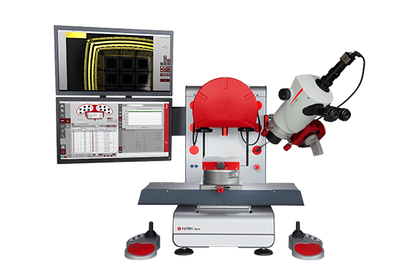
Sigma bond testers
Sigma bond testers are a revolutionary solution for measuring mechanical bond strength. The Sigma bond tester outshines all other bond testers with a remarkable 0.075% accuracy and a relative shear height precision of 200 nm. Enjoy the game-changing automation capabilities, including hands-free (un)loading and deep learning image processing for automatic testing and analysis. Your journey toward revolutionary bond testing begins here. If you have any questions or want to learn more, please don’t hesitate to reach out.\